Kioxia BiCS9 QLC to Bring 4-Bit NAND and Faster Interface to Consumers
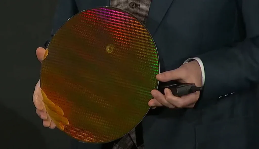
Kioxia is splitting its next-generation 3D NAND strategy between server-focused high-density flash and more cost-oriented parts for consumers. While its BiCS10 roadmap targets maximum storage density for the server market, the company says its BiCS9 line is intended to bring a faster interface to the consumer space—starting with a QLC option rated at 2 Tbit (256 GB) per die.
Key takeaways
- BiCS10 is positioned for the server segment with the highest-density BiCS flash, while BiCS9 targets consumer products.
- BiCS9 QLC is specified at 2 Tbit capacity per die, with 4 bits stored per flash cell.
- BiCS9 is a hybrid design: BiCS8-type memory cells paired with an I/O area that resembles BiCS10.
- The BiCS9 interface is claimed at 4.8 Gb/s, which Kioxia says is a 33% increase over BiCS8 generation devices.
- Kioxia has shared technical details for BiCS9 and BiCS10, but no concrete mass-production launch dates were provided.
BiCS9 is a hybrid of BiCS8 cells and BiCS10-like I/O
Kioxia’s BiCS9 architecture blends “old” and “new” elements rather than being a fully fresh cell design. The memory cells are based on the BiCS8 generation, but the die also includes an updated I/O section that aligns more closely with what Kioxia uses for BiCS10.
The company attributes this combination to a manufacturing technique introduced with BiCS8 called “CMOS directly Bonded to Array” (CBA). With CBA, two wafers are bonded together via wafer bonding, allowing the resulting die to pair different components efficiently.
As a result, BiCS9 is described as a 230-layer 3D NAND with an interface rate of 4.8 Gb/s. Kioxia says this interface speed is 33% faster than the BiCS8 generation, matching the interface target it associates with BiCS10. However, the company did not provide a specific figure for areal density for BiCS9, only noting that it should be closer to BiCS8 than to the density-leading BiCS10.
BiCS9 QLC: 2 Tbit per die, plus a promise of higher performance
Kioxia says it will offer both TLC and QLC versions for BiCS9. The QLC variant is specified at 2 Tbit per die, representing 4 bits per cell, while the TLC variant is positioned at 1 Tbit per die and 3 bits per cell.
Kioxia also highlights the typical trade-off of QLC: higher storage capacity can come at the cost of performance and endurance. Still, the company points to prior progress with QLC in the BiCS8 generation, where performance in real SSDs has improved substantially. It notes that SSDs such as the WD Blue SN5100 can lead performance within their class despite being built on BiCS8 QLC, with the biggest remaining weakness showing up mainly in prolonged write testing—something that may matter less depending on workload.
For BiCS9 QLC specifically, Kioxia claims additional performance improvements. One of the stated mechanisms is the 6-plane architecture of BiCS9, which is intended to raise read and write throughput.
In comparison to the prior 2 TB QLC approach from the BiCS8 generation, Kioxia says BiCS9 with the 6-plane design and other performance enhancements delivers higher write and read bandwidth. It also claims better energy efficiency for both writing and reading, alongside the same 4.8 Gb/s NAND interface speed. That interface figure is presented as a 33% improvement over BiCS8-era devices.
No public schedule for when BiCS9/BiCS10 will ship at scale
While Kioxia has provided technical specifics for both BiCS9 and BiCS10, it did not include concrete timelines for when mass production will begin. The first chips from these generations have been in sampling at least since July.
Overall, Kioxia’s approach for BiCS9 is presented as a cost-conscious upgrade path: reuse proven cell technology while improving the interface and internal performance characteristics. The company also describes its method as combining established storage-cell techniques with newer CMOS technology to achieve high performance without proportionally escalating investment costs.
Kioxia’s strategy also leaves room for future naming and pairing—suggesting that a later generation could mix the higher-density cell side of BiCS10 with the interface characteristics of a subsequent generation (for example, a BiCS11 concept using BiCS10 storage capacity and a BiCS12-style interface).